
Programme Timetable
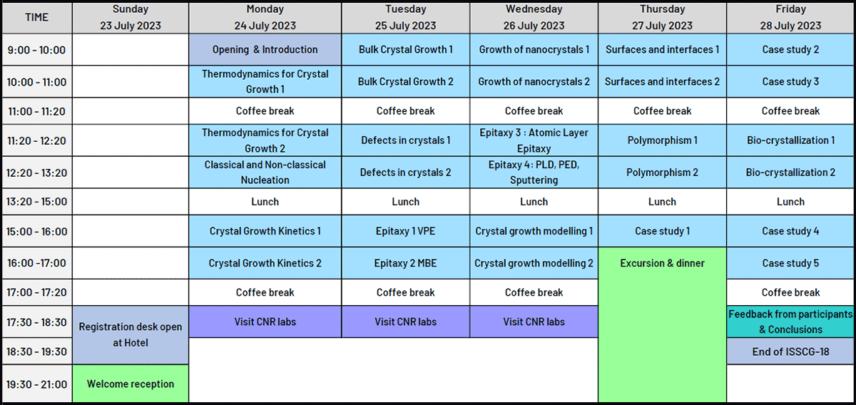
click on the image above to download the PDF file
Lectures & Lecturers
FUNDAMENTALS
• Thermodynamic aspects of crystal growth
Detlef Klimm, Leibniz IKZ, Berlin, Germany
Detlef Klimm, Leibniz IKZ, Berlin, Germany
Studied crystallography at Leipzig University, where he got the PhD and habilitation; worked on solid-state micromechanics and crystal defects in Moscow, Göttingen, and Tübingen; from 1996 at Leibniz-Institut für Kristallzüchtung (IKZ) Berlin where he established a thermo-analytic laboratory.
He mostly worked on oxide and fluoride materials (characterization, determination of phase diagrams) and is author of about 160 publications and book chapters, 2 textbooks, including "Thermal Analysis and Thermodynamics: In Materials Science (De Gruyter, 2022)". He was member of the IUCr "Commission on Crystal Growth and Characterization of Materials".
He mostly worked on oxide and fluoride materials (characterization, determination of phase diagrams) and is author of about 160 publications and book chapters, 2 textbooks, including "Thermal Analysis and Thermodynamics: In Materials Science (De Gruyter, 2022)". He was member of the IUCr "Commission on Crystal Growth and Characterization of Materials".
• Classical and non-classical nucleation
• Crystal growth kinetics
Alexander Van Driessche, CSIC, University of Granada, Spain
• Crystal growth kinetics
Alexander Van Driessche, CSIC, University of Granada, Spain
His research is focused on the fundamental aspects of (non)classical nucleation and growth processes in natural and engineered environments of a wide range of materials, including protein crystals, salt minerals and cementitious phases. A common thread in his work has been the application of in situ monitoring tools, such as advanced optical microscopy, atomic force microscopy, electron microscopy, and synchrotron based x-ray scattering techniques.
• Surfaces and interfaces
Elias Vlieg, Radboud University, Nijmegen, The Netherlands
Elias Vlieg, Radboud University, Nijmegen, The Netherlands
Professor of Solid State Chemistry at the Radboud University in Nijmegen, The Netherlands. The research theme of his group is the fundamental understanding of crystal growth, for which a wide range of experimental, computational and theoretical methods are applied to a wide range of crystals. His current interests include chiral separation, nanocrystals, co-crystals and the atomic-scale structure of solid-liquid interfaces. As head of the Applied Materials Science group, he is further involved in the practical applications of III-V semiconductors for thin film solar-cells.
• Crystal growth modelling
Jeff Derby, University of Minnesota, USA
Jeff Derby, University of Minnesota, USA
Distinguished McKnight University Professor, Department of Chemical Engineering and Materials Science, University of Minnesota, is a long-standing member of the crystal growth community. His research applies theoretical analysis and computational modeling to study continuum transport, mechanics, and phase change during the growth of large, single crystals. He has served as the President of the American Association for Crystal Growth (AACG) and is currently the Editor-in-Chief of the Journal of Crystal Growth. In 2015, he received the AACG Award “for Pioneering Contributions to Multiscale Modeling of Crystal Growth.”
• 1D, 2D, 3D defects in crystalline materials
Roberto Balboni, IMM-CNR, Bologna, Italy
Roberto Balboni, IMM-CNR, Bologna, Italy
Roberto Balboni graduated in Physics at the University of Bologna and is researcher at the Bologna site of CNR-IMM Institute, in Italy. He was at the Department of Physics of the University of Modena until 1993, then he moved to the Bologna section of CNR-IMM (formerly LAMEL Institute). His research activity has been devoted to the characterization of materials mainly using electron microscopy methods; this includes diffraction imaging and analysis, characterization of extended defects in semiconductors, high resolution imaging, phase analysis and spectroscopy of materials at the nanoscale. At CNR-IMM he contributed to the development of convergent beam diffraction analysis to the measurements of strain fields at the nanoscale in crystalline semiconductors. His recent activity includes the generation and study of electron beam shaping by means of holographic methods and the development of in-situ investigations in the TEM.
He was responsible for the Characterization Technological Section at CNR-IMM Institute from 2017 to 2019. He was the Director of five editions of the Electron Microscopy School in Materials Science in Bologna from 2008 to 2016. He is the President of the Italian Society for Microscopical Sciences since January 2020.
He was responsible for the Characterization Technological Section at CNR-IMM Institute from 2017 to 2019. He was the Director of five editions of the Electron Microscopy School in Materials Science in Bologna from 2008 to 2016. He is the President of the Italian Society for Microscopical Sciences since January 2020.
• Polymorphism
Lucia Maini, University of Bologna, Italy
Lucia Maini, University of Bologna, Italy
Associate professor at University of Bologna since 2014; her research is in the field of structural determination by X-ray diffraction techniques on single crystal and powders. Her studies are directed the polymorph screeening, structural and thermal characterization of Active Pharmaceutical Ingredients and organic molecules studied as new organic semiconductors. Furthermore, for years she has used mechanochemical syntheses to obtain new luminescent coordination polymers based on halides of Cu (I) and Ag (I). She is currently involved in European projects on History of Chemistry. She is active in the popularization of science and she leads the group: "Conoscere la chimica".
TECHNOLOGIES
• Bulk crystal growth
Roberto Fornari, University of Parma, Italy
Roberto Fornari, University of Parma, Italy
From 1981 to 2003 he was research scientist at CNR-IMEM Institute in Italy, then Director of Leibniz Institute for Crystal Growth and Professor at Humboldt University Berlin (2003 - 2013). Presently Full Professor of Condensed Matter Physics at Parma University, where he also serves as Vice-Rector for Research. He served in different scientific associations and was President of IOCG during 2010-16. His scientific activity was mainly focused on growth and investigation of semiconductor single crystals and epitaxial films. He is author/co-author of about 240 papers, about 180 in international journals and 60 in proceedings; 12 book chapters and invited reviews; holds 10 patents.
• Molecular Beam Epitaxy
• Atomic Layer Epitaxy, Sputtering, Pulsed Laser Deposition
Hiroshi Fujioka, University of Tokyo, Japan
• Atomic Layer Epitaxy, Sputtering, Pulsed Laser Deposition
Hiroshi Fujioka, University of Tokyo, Japan
Received a B.S. degree in industrial chemistry from the University of Tokyo, Japan, in 1984. He received the M.S. and Ph.D. degrees in materials science and mineral engineering from University of California, Berkeley, in 1993 and 1995 respectively. He was at Fujitsu Limited as a semiconductor engineer from 1984. In 1996, he joined the University of Tokyo and became professor at the Institute of Industrial Science in 2004. His research interests are in the areas of PLD, MBE, and sputtering growth of III-V semiconductors and their applications for high-speed electronic and optoelectronic devices. He has been serving as a president of Japanese Association of Crystal Growth from 2022. He has been also serving as chairman of the Japan Society for the Promotion of Science, R032 committee on crystal growth for industry innovations from 2021.
• Vapour Phase Epitaxy
• Growth of nanocrystals
Nicola Lovergine, University of Salento, Lecce, Italy
• Growth of nanocrystals
Nicola Lovergine, University of Salento, Lecce, Italy
Associate Professor in Solid State and Semiconductor Physics at the Department of Innovation Engineering, University of Salento, Italy. He received the PhD in Physics in 1991 from the University of Bari, Italy. His research interests focus on the physics and growth of III-V and II-VI compound semiconductors with emphasis on their applications to nano-photonic/nano-electronic devices, solar cells, and radiation detectors; MOVPE/VPE (nano)epitaxy of semiconductor hetero-structures and related (nanoscale) physical characterization methods. He has authored/co-authored over 150 publications in refereed journals, book chapters and conference proceedings, and has given several invited talks and lectures at international conferences/workshops and schools.
• Bio-crystallization
Monika Spano, Institute of Structural Biology, Grenoble, France
Monika Spano, Institute of Structural Biology, Grenoble, France
Associated Professor (Université Grenoble Alpes, France) she develops new assays for protein crystallography in the Synchrotron Group at the Institut de Biologie Structurale (IBS) (link) that developed the first plate screener at the European Synchrotron Radiation Facility. These mainly focus on (i) controlling and monitoring the crystallisation process (nucleation and crystal growth), (ii) crystallisation optimisation based on phase diagram investigation and (iii) microfluidic protein crystallisation regarding in situ diffraction and scattering methods. She also uses neutrons (as opposed to the more common X-rays) for structural studies addressing questions of biological significance.
CASE STUDIES
• Case study 1: Crystal growth and defect engineering of silicon
Joel Kearns, NASA Cleveland, USA
Joel Kearns, NASA Cleveland, USA
He is Deputy Associate Administrator for Exploration at NASA’s Science Mission Directorate in Washington, DC. He leads NASA scientific planning for astronaut missions beyond low earth orbit, as well as NASA’s Lunar Discovery and Exploration Program (LDEP) including scientific investigations, commercial lunar payload services (CLPS), scientific instruments for Artemis lunar astronauts. His research interests are in phase transformations, particularly single crystal growth and defects in silicon, electron microscopy and spectroscopy, and x-ray diffraction. He was Vice President for Solar R&D at MEMC Electronic Materials and Vice President for Engineering and Technology at SUMCO USA, where he focused on crystal growth and defect engineering of silicon.
• Case study 2: Artificial Intelligence in crystal growth
Natasha Dropka, Leibniz IKZ, Berlin, Germany
Natasha Dropka, Leibniz IKZ, Berlin, Germany
She graduated in Chemical Engineering at the University of Novi Sad, where she received her Magister and DrSc degrees in cooperation with University College London and Faculty of Chemical Technology in Prague. She worked at the Faculty of Technical Sciences in Novi Sad, at the Leibniz Institute for Catalysis in Berlin. Since 2008 she is research scientist at the Leibniz Institute for Crystal Growth in Berlin where she is currently heading the Fundamental Description Section with research interests in machine learning and CFD simulations of crystal growth processes.
• Case study 3: Growth of 2-dimensional crystals
Joan Redwing, Penn State University, USA
Joan Redwing, Penn State University, USA
Distinguished Professor of Materials Science and Engineering at Penn State University and serves as Director of the 2D Crystal Consortium Materials Innovation Platform– a national user facility funded by the U.S. National Science Foundation that is focused on advancing the synthesis of 2D materials for next generation devices. Her research focuses on crystal growth and epitaxy of electronic materials, with an emphasis on thin film and nanomaterial synthesis by metalorganic chemical vapor deposition (MOCVD). She currently serves as vice president of the American Association for Crystal Growth, is an associate editor for the Journal of Crystal Growth and is the North American Regional editor for the journal 2D Materials. She is a fellow of the American Physical Society, Materials Research Society and the American Association for the Advancement of Science. She is an author/co-author of over 300 publications in refereed journals and holds 8 U.S. patents.
• Case study 4: Horizontal Liquid Phase Transport of oxides
Jiaqiang Yan, Oak Ridge National Laboratory, TN, USA
Jiaqiang Yan, Oak Ridge National Laboratory, TN, USA
He received his B.E. and M.E. at Northeast University in China in 1992 and 1994, respectively, and the Ph.D. in Materials Science and Engineering in 2004 at University of Texas, Austin. His research interests include design and synthesis of novel materials, mainly in single crystal form; structure, chemistry, and property relationship in correlated quantum materials; electrical, magnetic, and thermal properties of correlated quantum materials.
He is presently at Oak Ridge National Lab and Joint Associate Professor at University of Tennessee, Knoxville; before he has been Postdoctoral Research Associate and Assistant Scientist, Division of Materials Science and Engineering, Ames Laboratory, Ames, IA. He his author/co-author of about 300 papers in refereed journal and is Clarivate Highly Cited Scientist from 2019. Member of American Physical Society, American Association for Crystal Growth, American Ceramic Society. Among several awards, he got the Outstanding Research Accomplishment Award, MSTD, ORNL, 2022.
He is presently at Oak Ridge National Lab and Joint Associate Professor at University of Tennessee, Knoxville; before he has been Postdoctoral Research Associate and Assistant Scientist, Division of Materials Science and Engineering, Ames Laboratory, Ames, IA. He his author/co-author of about 300 papers in refereed journal and is Clarivate Highly Cited Scientist from 2019. Member of American Physical Society, American Association for Crystal Growth, American Ceramic Society. Among several awards, he got the Outstanding Research Accomplishment Award, MSTD, ORNL, 2022.
• Case study 5: Needs and perspectives of industrial crystal production
David Callejo Munoz, SiCreate, Leonding, Austria
David Callejo Munoz, SiCreate, Leonding, Austria
After the study of physics and material science, with focus on crystal growth in Madrid Autonoma University, he started his industrial activity in 2002. He created and scaled up a production line for Lithium Niobate in Italy, and then a Scintillator and laser crystals production line between Italy and USA.
From 2008 he also acted as external technical responsible for many industrial crystal growth projects worldwide, mainly about sapphire, with projects in China, Korea and Taiwan. One of the biggest challenges as technical responsible was the Apple-GTAT project with more than 2000 HEM sapphire crystal growth furnaces in Arizona, USA.
He is consulting for the most important crystal producers, as board advisor and strategic consultant. His last adventure, Sicreate GmbH, unfolds around silicon carbide raw material for SiC crystal growth. It is a patented technique with a circular economy and sustainable approach for an European semiconductor supply chain.
Your account
LAST UPDATES:
- Programme timetable has been updated
- ISSCG18 started!
- Contact list is now available in your "Reserved area"
- The official booklet with abstracts of all ISCCG18 lectures is now available for download in your "Reserved area"
- Updated Info has been uploaded to your "Reserved area". Further updates and school material coming soon.
SPONSORED BY:

Copyright © 2022 ISSCG18
web creation & design: Davide Calestani